The findings, led by researchers from the University of Cambridge, are published in the journal Nature Nanotechnology.
The most commonly used material for producing solar panels is crystalline silicon, but achieving efficient energy conversion requires an energy-intensive and time-consuming production process to create a highly ordered wafer structure.
In the last decade, perovskite materials have emerged as promising alternatives to silicon.
The lead salts used to make perovskites are much more abundant and cheaper to produce than crystalline silicon, and they can be prepared in liquid ink that is simply printed to produce a film of the material. They also show great potential for other applications, such as energy-efficient light-emitting diodes (LEDs) and X-ray detectors.
The performance of perovskites is surprising. The typical model for an excellent semiconductor is a highly ordered structure, but the array of different chemical elements in perovskites creates a much ‘messier’ landscape.
This messiness causes defects in the material that lead to tiny ‘traps’, which typically reduce performance. But despite the presence of these defects, perovskite materials still show efficiency levels comparable to their silicon alternatives.
In fact, earlier research by the same team behind the current work showed the disordered structure can actually increase the performance of perovskite optoelectronics, and their latest work seeks to explain why.
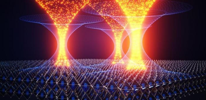
Combining a series of new microscopy techniques, the group present a complete picture of the nanoscale chemical, structural and optoelectronic landscape of these materials, that reveals the complex interactions between these competing factors and ultimately, shows which comes out on top.
“What we see is that we have two forms of disorder happening in parallel,” said first author Kyle Frohna from Cambridge’s Department of Chemical Engineering and Biotechnology (CEB). “The electronic disorder associated with the defects that reduce performance, and then the spatial chemical disorder that seems to improve it.
“And what we’ve found is that the chemical disorder – the ‘good’ disorder in this case – mitigates the ‘bad’ disorder from the defects by funnelling the charge carriers away from these traps that they might otherwise get caught in.”
Image: Artistic representation of electrons funneling into high quality areas of perovskite material
Credit: Alex T. at Ella Maru Studios
Reproduced courtesy of the University of Cambridge